Research Note · Measurement Infrastructure
From Simulation to Hardware: The Measurement Board Is Finally Designed
The measurement platform is ready to move from PCB design to experimental validation
The schematic and PCB layout are complete, the board has been fabricated, and the next phase is to validate a controlled platform for measuring MLCC distortion under DC bias.
The schematic and PCB layout are complete, the board has been fabricated, and the remaining components are awaited before assembly and validation.
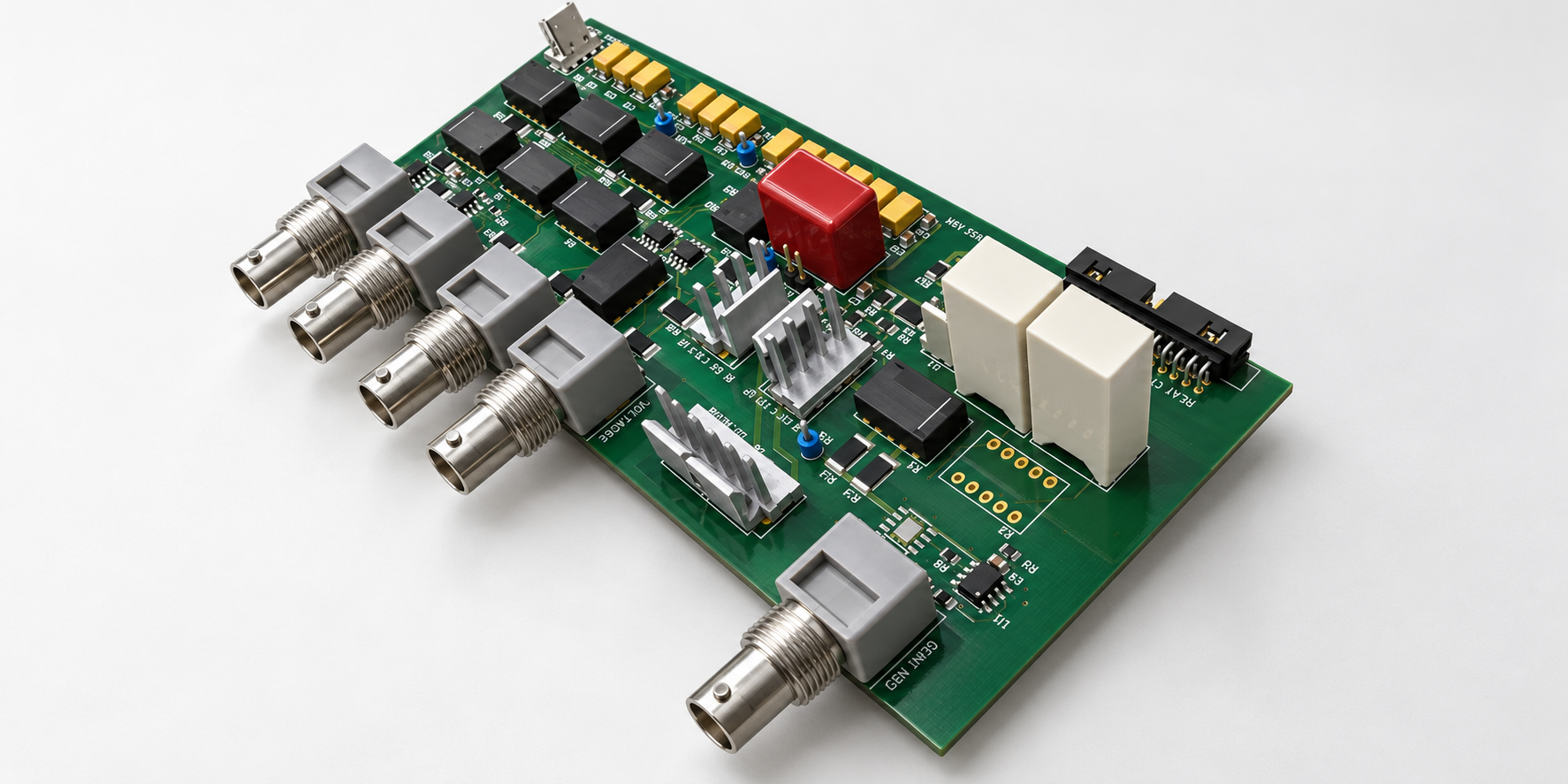
This project took longer to design than I expected.
That usually happens when a measurement problem looks simple on paper.
The original goal was straightforward: build a small test platform that would let me measure the nonlinear distortion generated by ceramic capacitors under different DC-bias conditions and compare the results with the models I had developed earlier.
At first, I expected the hardware to be the relatively easy part.
It was not.
The electrical design is now complete, the PCB has been fabricated, and the board itself is already sitting on my desk. The render shown here represents the fully populated version of the design.
At the moment, the project is in the least exciting phase of hardware development: waiting for parts.
Some of the components have fairly long lead times, so assembly will have to wait a little longer. But the important part is that the design is finished and the project is moving from simulation and measurement-system development toward real hardware.
What this board is for
The purpose of the system is to characterize nonlinear distortion in ceramic capacitors, primarily MLCCs, under controlled operating conditions.
The specific question I am interested in is how capacitor nonlinearity changes with DC bias and how that behavior shows up as distortion in otherwise simple passive circuits.
That sounds like a small problem.
In practice, it is not.
High-permittivity ceramic capacitors such as X7R devices are not perfectly linear components. Their capacitance changes with applied voltage, and once that voltage dependence becomes part of the signal path, the capacitor behaves as a weak nonlinear element.
In a passive RC network, that nonlinearity can generate harmonic distortion.
Earlier parts of this work were focused mainly on analysis and simulation. I worked with vendor C-V data, developed nonlinear charge-voltage models, and used those models to estimate the distortion that should appear in passive filters.
The obvious next step was experimental validation.
That meant building a measurement setup capable of resolving distortion levels that may be very small.
And that is where the project became much more interesting.
The real problem is the measurement system
If you are measuring large signals, the setup can be simple.
If you are trying to measure very small nonlinear products, the test fixture itself becomes part of the experiment.
It is no longer enough to connect a signal generator, a capacitor, and an analyzer and assume that whatever appears in the spectrum came from the device under test.
The system has to answer a more difficult question:
How much of the measured distortion comes from the capacitor, and how much comes from the measurement setup itself?
That affects almost every design decision.
The board has to provide a controlled way to inject DC bias without corrupting the AC measurement path. It has to support different test configurations. It has to keep switching elements, protection circuitry, passive components, routing, and grounding from introducing distortion at a level comparable to the effect being measured.
Parasitics matter.
Leakage matters.
Relay or switch behavior matters.
Grounding matters.
Component selection matters.
Even the way the signal path is physically laid out can become important when the quantities of interest are small enough.
The board therefore evolved from a simple test adapter into a dedicated measurement platform.
DC bias made the problem more complicated
One of the main requirements is to measure the same capacitor at different DC operating points.
That is important because the electrical field inside an MLCC affects its effective capacitance and, more importantly for this project, its nonlinear behavior.
The DC bias therefore has to be applied in a controlled way while keeping the analyzer and signal source within their intended operating conditions.
The bias network also has to be sufficiently linear itself.
Otherwise, it becomes very easy to build a system that measures the distortion of the bias circuitry rather than the distortion of the capacitor.
This is one of the reasons the design took longer than expected.
Every additional circuit element added for convenience, protection, or switching also becomes a possible contributor to the measurement result.
That is not a problem that can be solved only by simulation. At some point, the complete system has to be built and characterized.
Establishing the system floor comes first
The analyzer used in this project is a QuantAsylum QA403.
It provides the kind of functionality I need for this work: low-distortion signal generation, differential acquisition, spectral analysis, automated sweeps, and programmatic control.
But the analyzer specification alone does not define the usable measurement floor of the complete setup.
The first real task after board bring-up will therefore not be measuring X7R capacitors.
It will be measuring the measurement system.
I want to establish a clean loopback baseline and then characterize the complete signal path through the test board in several configurations.
Only after that will it be possible to say what distortion levels can actually be attributed to the device under test.
This baseline will also tell me which experiments are realistic.
For example, I expect C0G/NP0 capacitors to be useful as a control because their voltage coefficient and nonlinear behavior are much smaller than those of X7R parts.
There is a good chance that, under some conditions, the distortion from a C0G capacitor will simply disappear below the floor of the measurement setup.
That is not a failed measurement.
It is useful information about the capability of the system.
What I plan to measure
One of the first comparisons will be between X7R capacitors with different voltage ratings.
For example, a 6.3 V X7R device and a 50 V X7R device may have the same nominal capacitance, but electrically they are not necessarily equivalent once DC bias is applied.
The internal dielectric structure and electric-field conditions can be very different.
The plan is to repeat measurements across several DC-bias levels and observe how the distortion changes with operating point.
The first measurement campaign will likely include:
- loopback and system-floor characterization;
- comparison of X7R parts with different voltage ratings;
- measurements at multiple DC-bias levels;
- C0G/NP0 parts as a linearity reference;
- comparison of measured results with the nonlinear models developed earlier.
The interesting part will not be a single THD number.
What matters is the trend.
If the model predicts that distortion should increase in a certain way with bias, frequency, or signal amplitude, does the real component actually behave that way?
That is the experiment I want to run.
Automation is part of the design
Another important part of the project is repeatability.
A useful measurement campaign cannot rely on manually changing settings, taking screenshots, and writing numbers into a spreadsheet.
There are too many variables.
Frequency, AC signal level, DC bias, capacitor type, voltage rating, test topology, and measurement bandwidth can all change from one run to another.
Even a modest test matrix quickly becomes hundreds of measurements.
So from the beginning, I have treated automation as part of the measurement architecture rather than as an optional convenience.
The QA403 is especially useful here because it can be controlled through a local HTTP API.
That makes it possible to automate sweeps, retrieve measurement results, collect raw time-domain and frequency-domain data, and process the data directly in software.
The goal is to make the experiment reproducible.
Ideally, a complete test series should be something that can be described by a script, repeated later, and compared directly against the simulation results using the same analysis pipeline.
That is much more valuable than a one-off measurement.
Where the project stands now
The schematic is complete.
The PCB layout is complete.
The board has been fabricated.
The image shown in this post is a render of the fully assembled design, while the bare PCB itself is already here.
Now I am waiting for the remaining components.
Once the parts arrive, the next phase will be standard hardware bring-up:
power checks, functional checks of individual sections, verification of the switching paths, validation of the DC-bias circuitry, and finally characterization of the complete measurement chain.
Only after that will I start the capacitor measurements.
There is still plenty that can go wrong.
A board can look perfect in CAD and still have a wiring mistake, an incorrect component value, an unexpected parasitic path, or a layout issue that only becomes obvious on real hardware.
That is why I do not consider the design finished just because the PCB files are finished.
For measurement hardware, validation is part of the design process.
The project will be open source
I plan to release the complete project on GitHub.
That will include the schematic, PCB files, and the supporting information needed to reproduce the hardware.
But I will only publish the design after the board has been assembled, tested, and validated.
I do not want to release an unverified hardware design and present it as complete.
There is a meaningful difference between a schematic that appears correct and a board that has been built, measured, and demonstrated to work as intended.
So the sequence will be simple:
build it, test it, fix whatever needs fixing, validate the measurement performance, and then publish the design.
The interesting part starts next
Up to this point, most of the work has been about models, simulations, circuit architecture, and measurement-system design.
The next phase is where the project becomes physical.
Real capacitors.
Real bias voltages.
Real spectra.
And, hopefully, a meaningful comparison between theory and measurement.
The project turned out to be more complicated than I expected when I started.
That also made it much more interesting.
Now I am looking forward to seeing whether the hardware — and the models behind it — behave the way I expect.
Work continues.