MLCC Distortion Meter · Engineering Note 001
Measuring MLCC Distortion Under DC Bias
A two-channel system architecture
Distortion in the measured capacitor current can originate in the generator, output stage, bias network, or measurement path. The architecture therefore records the actual MLCC voltage and current simultaneously while applying DC bias.
The signal paths and the purpose of each major block are defined. Circuit implementation, component values, calibration, and the final analysis algorithm remain subjects of later engineering notes.
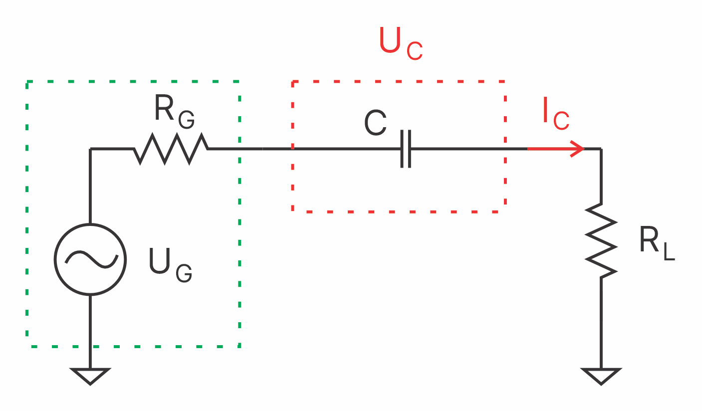
The measurement path starts with a series circuit: a signal source, the MLCC under test, and a current-sense resistor. Testing a Class 2 MLCC adds three constraints. The capacitor must operate under DC bias, its voltage must be measured directly across its terminals, and the test setup must contribute less distortion than the device under test.
Why measure voltage and current at the same time?
An MLCC is a two-terminal device. The generator setting U_G is not necessarily the voltage that appears across those terminals. Some of the applied voltage drops across the series impedances, and the output stage can introduce gain error, phase shift, and distortion. The instrument therefore records both the actual capacitor voltage U_C and the capacitor current I_C.
For an ideal linear capacitor, current is given by
If the voltage is sinusoidal and the capacitance is constant, the current is sinusoidal as well. In a nonlinear dielectric, charge is no longer proportional to voltage, so the more useful relationship is i(t) = dq(u)/dt. The current can then contain additional harmonics even when the voltage remains close to a sine wave.
Source and driver harmonics appear first in U_C and then in I_C. A current-only measurement could incorrectly attribute them to the MLCC. Capturing both signals gives the analysis the actual amplitude, phase, and waveform applied to the DUT.
Adding DC bias without back-driving the source
The effective capacitance of a Class 2 ceramic capacitor depends on both DC and AC voltage. DC bias sets the operating point on the nonlinear charge-voltage curve; sine-wave amplitude determines how far the device moves around that point during each cycle.
The external bias voltage cannot simply be tied to the QA403 output. The source must be isolated from DC, while the test circuit still needs enough AC drive current. The output buffer, coupling capacitor C_D, and bias-injection network perform those jobs.
The buffer presents a light load to the QA403 and supplies the required test current. C_D passes the AC stimulus while blocking DC from the buffer and generator. The bias supply U_DCB feeds the test node through R_DCB, which provides a charging path and limits AC current into the bias supply.
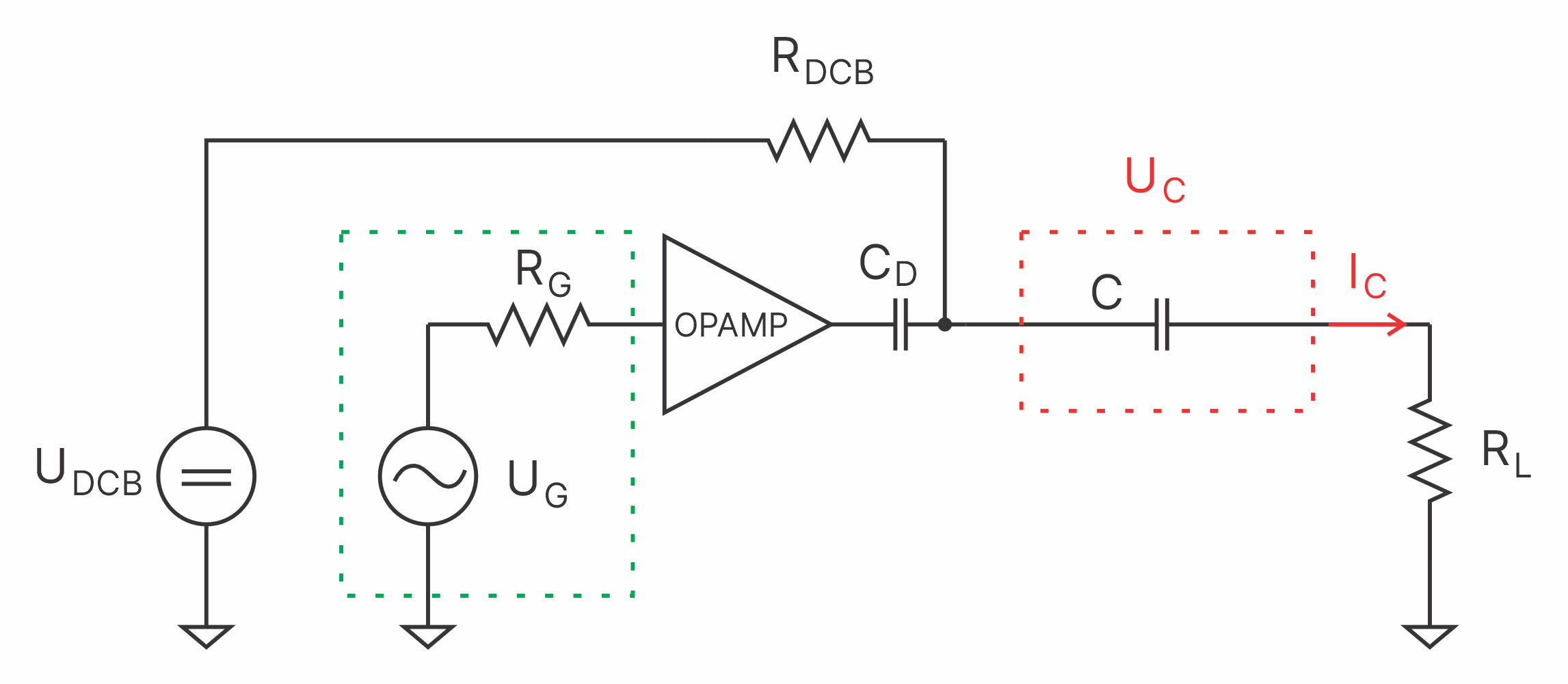
The impedance of the R_DCB branch, including the bias supply output impedance, must remain high enough across the measurement band. Otherwise, some AC current will be diverted into the bias supply instead of flowing through the DUT.
The coupling capacitor is part of the measurement path. Its capacitance, dielectric, voltage rating, frequency response, and residual nonlinearity all affect measurement accuracy.
Measuring the capacitor voltage differentially
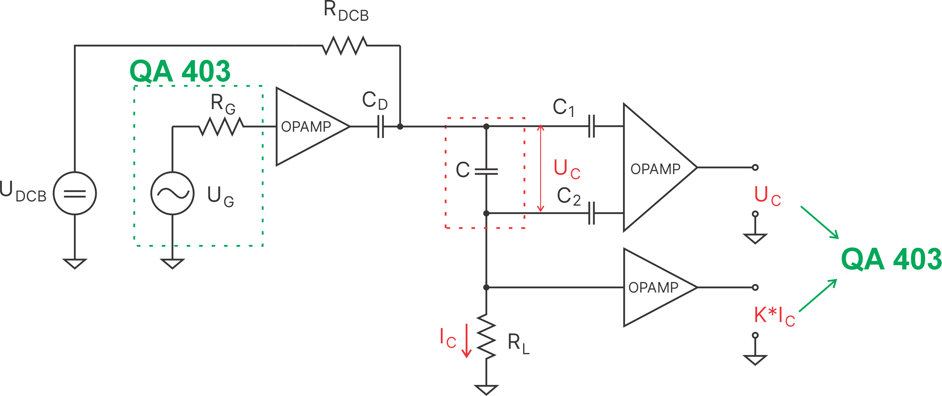
The lower DUT terminal connects to R_L, not directly to ground. The MLCC voltage is
A single-ended measurement of the upper terminal would include the voltage across the current-sense resistor. The voltage channel must measure the difference between the two capacitor terminals.
Figure 3 shows C_1, C_2, and a differential buffer ahead of the voltage channel. Channel accuracy depends on matching the full complex impedance of both legs across the measurement band—not just nominal capacitance. Input resistance, phase shift, leakage, and voltage-dependent capacitance all matter.
The triangle represents the function of the voltage channel, not a committed circuit implementation. The detailed input-stage design will determine the required DC-fault protection, scaling, input impedance, and isolation.
Converting capacitor current into a voltage
If the voltage channel has sufficiently high input impedance, essentially all capacitor current flows through R_L. The shunt voltage is
With current-channel amplifier gain A_I, the output becomes
Figure 3 labels this output as K × I_C, where K is the overall transimpedance in volts per ampere. It includes R_L, analog gain, and any later calibration factor.
Increasing R_L improves sensitivity but also raises the shunt voltage and reduces the voltage left across the MLCC. A smaller shunt interferes less with the test condition, at the cost of a lower signal and a more demanding low-noise amplifier.
Using the QA403 as source and acquisition engine
The QA403 generates the stimulus and records both measurement channels. One input receives the signal proportional to the actual capacitor voltage U_C; the other receives K × I_C. Both waveforms and spectra are available from the same acquisition.
These labels refer to calibrated representations of the physical quantities. Coupling capacitors, input impedances, the current shunt, and amplifiers all sit between the DUT and the acquired data. Calibration must account for their amplitude and phase response.
Higher frequency demands more from the driver
Capacitive reactance falls as frequency rises. For a fixed sinusoidal voltage, current through a linear capacitor increases approximately as
The driver will hold the requested MLCC voltage only while it can supply that current. Near its limits, voltage drop across the output impedance, R_G, and R_Lbecomes more significant. Current limiting or insufficient slew rate can reduce U_C and distort its waveform.
At the low end of the band, C_D, C_1, and C_2 form high-pass networks with surrounding resistances. At the high end, usable bandwidth is limited by output current, active-stage speed, and measurement-channel response.
The test setup must be more linear than the DUT
The output buffer, coupling capacitor, bias network, shunt, differential voltage channel, and current amplifier can all generate distortion. If their contribution is comparable to the MLCC contribution, the analyzer measures the combined test setup rather than the capacitor alone.
Before comparing MLCCs, the setup needs a baseline: noise and residual-distortion measurements, a suitably linear reference device, and amplitude-and-phase characterization of both channels. These measurements will form a separate calibration procedure.
DC bias also introduces safety requirements. Coupling and protection components need adequate voltage ratings, stored charge must be discharged in a controlled way, and faults in the output buffer or bias supply must not reach the analyzer or DUT.
Architecture outcome
Four functions now have separate error budgets
The design separates AC generation, DC-bias injection, differential DUT-voltage measurement, and current-to-voltage conversion. Each path can now receive its own level range, bandwidth, error budget, and residual-distortion target.